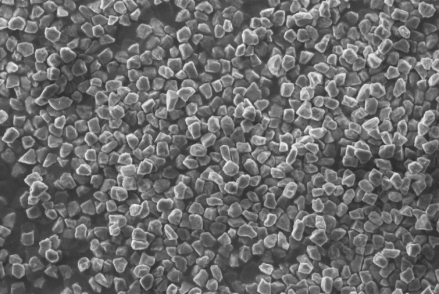
Core Advantages
Ultra-Precise Morphology Control:
Customized crystal shapes tailored to client requirements, balancing "sharpness" and "flatness" for different processes. Enhances machining efficiency and achieves nanometer-level precision.
High Purity & Non-Magnetic:
Proprietary purification technology and strict material selection minimize metallic impurities (e.g., Fe, Ni, Co). Magnetic-free properties ensure critical protection for wafer yield.
Strict Oversized Particle Control:
Patented technology eliminates oversized particles, preventing scratches and defects during processing.
Narrow Distribution & Superior Dispersion:
Tight particle size distribution with excellent dispersibility and strong bonding to substrate materials.
Standardization & Consistency:
SOP-controlled production, data/sample archiving, dynamic client profiles, and dual stability verification ensure batch-to-batch reliability.
Available Particle Size Specifications:
Conventional Fine Diamond Powder(μm) |
0-0.2 | 0-0.25 | 0-0.5 | 0-1 | 0.5-1 |
0-2 | 1-2 | 1-3 | 2-3 | 2-4 |
2-5 | 3-5 | 4-6 | 4-8 | 5-10 |
6-12 | 8-12 | 8-16 | 10-20 | 20-30 |
20-40 | 30-40 | 40-50 |
|
|
Nano Diamond Powder |
20 | 30 | 50 | 80 | 100 |
Tianjian Deep Customization Services:
To address the precise requirements of semiconductor cutting, grinding, and polishing processes, Tianjian goes beyond standard fine powder supply. By integrating material
expertise with technical guidance, we deliver fully tailored solutions for each stage of your workflow.
Application:
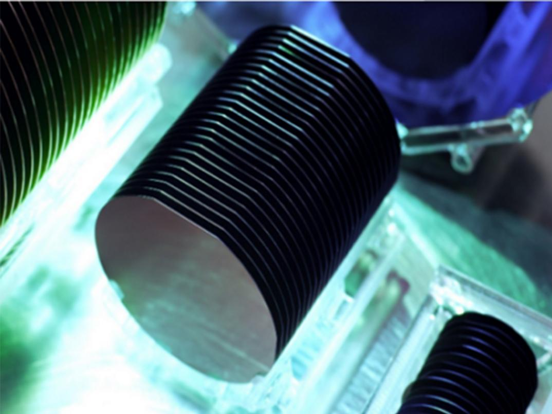
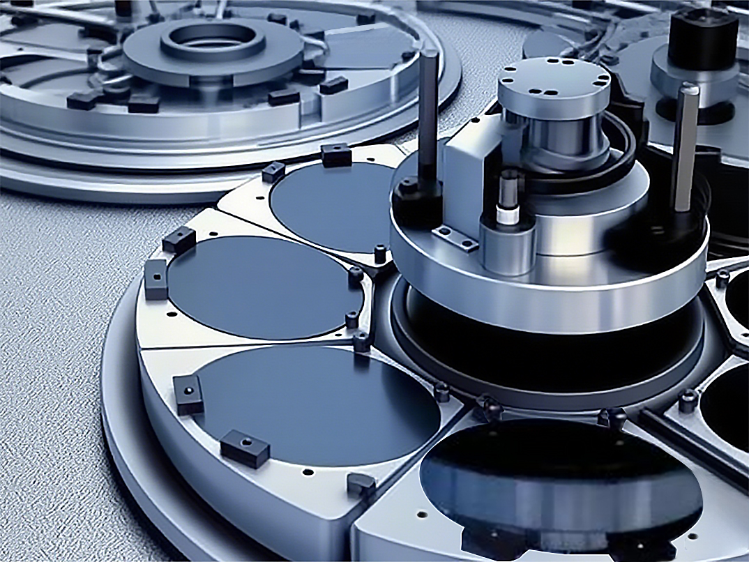
Silicon Carbide Seed Crystal Lapping;Silicon Carbide Wafer Processing;Magnetic Head/Resistance Polishing;Electronic Component Polishing

 English